
NXP 74LV4052PW: A Comprehensive Technical Overview of the Dual 4-Channel Analog Multiplexer/Demultiplexer
The NXP 74LV4052PW is a high-performance, dual 4-channel analog multiplexer/demultiplexer integrated circuit designed with low-voltage operation and versatile signal routing capabilities. Fabricated using advanced silicon-gate CMOS technology, this device is engineered to handle both analog and digital signals, making it a fundamental component in a wide array of electronic systems, from data acquisition and audio routing to communication interfaces and test equipment.
A key feature of the 74LV4052PW is its dual independent 4:1 multiplexer/demultiplexer configuration. Each of the two switches can select one of four input channels and connect it to a common output, or conversely, route a common input to one of four outputs—functioning perfectly as both a mux and a demux. This bidirectional capability is essential for applications requiring flexible signal path management. The device includes two binary control inputs (A and B) and an active-low enable input (E̅). The logic levels applied to these inputs determine which channel is connected, allowing straightforward digital control of analog signals.
The IC operates across a wide supply voltage range from 1.0 V to 5.5 V, making it fully compatible with modern 3.3V and 5V logic systems, and even suitable for battery-powered, low-voltage devices. Despite its low-voltage nature, it can handle analog signals that swing up to the supply rails. A significant advantage is its very low "on" resistance, which is relatively flat across the entire signal range, minimizing distortion and signal attenuation. Furthermore, the device boasts extremely low quiescent current and very low switch-off leakage current, ensuring minimal power consumption—a critical factor for portable and power-sensitive applications.
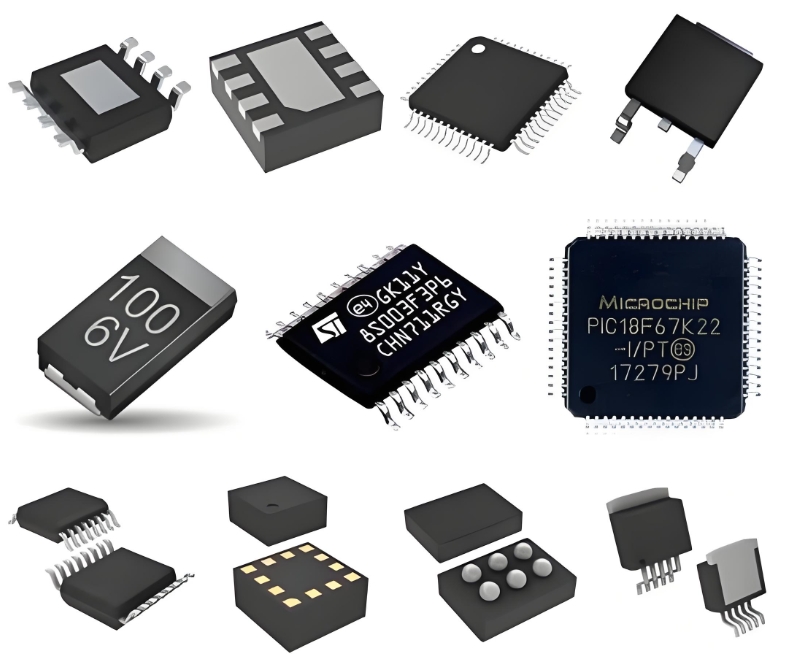
The 74LV4052PW is offered in a TSSOP-16 (Thin Shrink Small Outline Package), identified by the "PW" suffix. This surface-mount package provides a compact footprint, which is ideal for high-density PCB designs. The device is specified for operation over a broad temperature range from -40°C to +125°C, ensuring reliability in industrial and automotive environments.
ICGOOODFIND: The NXP 74LV4052PW stands out as an exceptionally versatile and efficient solution for analog and digital signal switching. Its combination of low-voltage operation, minimal power consumption, and robust performance makes it an excellent choice for designers seeking reliability and flexibility in signal routing applications.
Keywords: Analog Multiplexer, Low-Voltage CMOS, Bidirectional Switch, Low On-Resistance, TSSOP-16 Package.

